Nanomaterials PECVD reactor

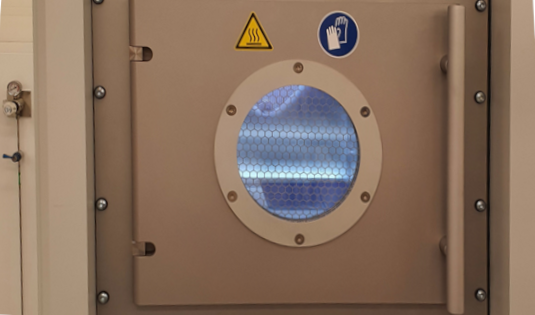
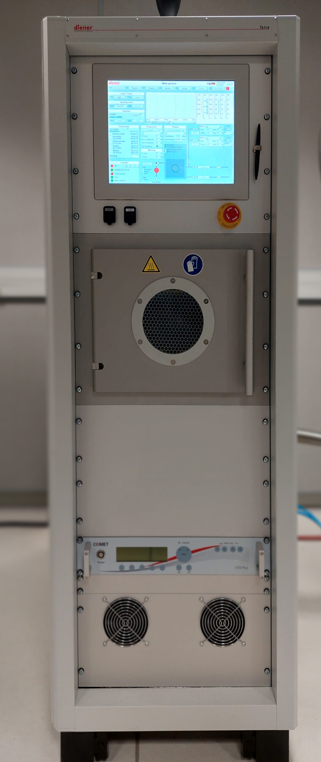
01Plasmacleaner: Diener tetra 30
Parameters
- Layer engineering / deposition systems
- PECVD CentroTherm with 4 quartz process chambers with a diameter of 210 mm and a length of 2000 mm
- Processing capacity for standard silicon wafers 15.6 cm x 15.6 cm in case of deposition of 500 nm Al2O3 – 1500 wafers / h
PECVD (plasma enhanced chemical vapour deposition) – a method that allows to carry out the coating / deposition process on substrates / objects / substrates at a temperature lower than classic CVD. The process consists of introducing gaseous substrates between two electrodes (one of them has a heated surface on which the deposition is carried out, the other is powered by waves with a frequency in the range of 40 kHz – 2.45 GHz).
Due to the ionization of gases in the electric field between the electrodes, it is possible to coat / deposit a specific layer on substrates sensitive to high temperatures at temperatures from 250 ° C to 350 ° C. Gas mixtures enable creation of following layers: silicon nitride, silicon oxide, silicon oxynitride, silicon carbide, amorphous silicon and others.
