Projekty Silicon-free cell
Projekty
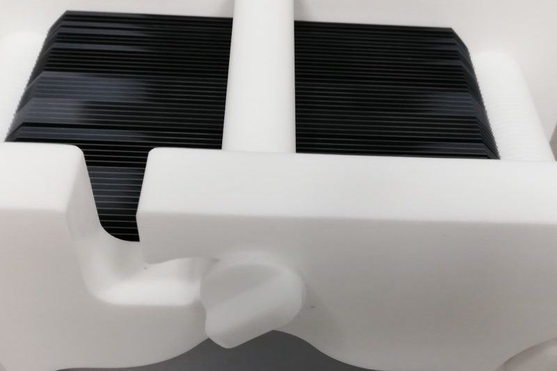
Development of a technology for producing functional materials for silicon-free photovoltaic cells
Data28/04/2022
Nazwa projektuFotowoltaika
AutorCBRTP
01Project description
The project involves the development of materials necessary to produce a silicon-free and double-sided photovoltaic cell and the preparation for the implementation of technology for their production. The designed cells will be made on perforated metal substrates (Cu / Al), on which semiconductor layers will be produced on both sides. Developed by CBRTP and protected by a patent application, the technology of producing semiconductors based on thermal copper oxide CuO obtained on a substrate, and at the same time, a Cu electrode allows to achieve ohmic contact Cu / CuO and on the Al substrate also acting as an electrode based on SnS tin sulphide, obtained in the CBD process, in both cases covered with an n-type semiconductor with the use of zinc oxide in the form of nanorods covered with a ZnMgO/AZO layer in the ALD process. Due to the nature of the oxidation, ALD, CBD and hydrothermal processes, a semiconductor structure on both sides of the cell is obtained in one cycle of processes. The project also involves the development of a technology for the production of perforated metal substrates in which the voids in the substrate will be filled with a dispersing medium in the form of a polymer with suspended metal particles, which will allow for the effective development of the cell's active surface. The project assumes both the selection of the perforation technique and the type of scattering medium, in co-operation with external research centres.
The produced cell materials/components will be characterised in terms of electrical, tribological and dilatometric properties as well as structure and morphology.
Finally, the manufactured cells will be subjected to metallisation, which will form an AZO cell with the upper layer (low-resistive ohmic contact). Due to the materials used in the cell, this process will be low-temperature so that the layers of the structure are not degraded. Therefore, metallic electrical contacts based on silver Ag particles and nanoparticles are planned on the transparent layer, as part of which the process will involve the development and production of heterophasic suspensions - inks compatible with this technology. The basis of the process will be to transform the ink into an aerosol mist, and then concentrate it and direct it towards the substrate in the form of a micrometre stream. Electrical contacts will constitute the electrode and will be applied by means of aerosol printing and embedded using low-temperature heat treatment techniques (up to 300ºC).
Another important factor is the goal prescribed for the tasks of the industrial partner, defined as striving to develop a process and tools for the assembly of photovoltaic modules with the use of a conventional machine park as part of research work, with particular emphasis on the SmartWire line at the partner's disposal. As part of the research work of the industrial partner, it was planned to develop the design and components for the distribution of foil and wire tapes based on standard machines provided by the manufacturer MeyerBurger AG, for full compatibility and the possibility of retooling the line, enabling the use of both conventional cells and those designed under this silicon-free cells project. The modules consisting of the developed silicon-free cells will be marketed by Hanplast and its representatives in Poland, the US, Ukraine, and Georgia, as well as in the course of market expansion throughout the EU.
The project is executed in connection with the agreement for co-financing of project No.TECHMATSTRATEG2/409122/3/NCBR/2019.
02Members of the scientific and industrial consortium
- Centrum Badań i Rozwoju Technologii dla Przemysłu S.A. – Consortium leader
- Instytut Metalurgii i Inżynierii Materiałowej im. Aleksandra Krupkowskiego Polskiej Akademii Nauk w Krakowie
- Instytut Metalurgii i Inżynierii Materiałowej im. Aleksandra Krupkowskiego Polskiej Akademii Nauk w Krakowie
03Project data
Execution period: 01.01.2019 – 31.05.2022
Total eligible project cost: PLN 17 550 437
Industrial research: PLN 14 467 545
R&D: PLN 2 169 092
Prace pzedwdrożeniowe: PLN 913 800
Amount of co-financing: PLN 15 213 307
Industrial research: PLN 12 797 045
R&D: PLN 1 593 842
Prace przedwdrożeniowe: 822 420 zł
Own contribution: 2 337 130 zł
Total eligible project cost: PLN 17 550 437
Industrial research: PLN 14 467 545
R&D: PLN 2 169 092
Prace pzedwdrożeniowe: PLN 913 800
Amount of co-financing: PLN 15 213 307
Industrial research: PLN 12 797 045
R&D: PLN 1 593 842
Prace przedwdrożeniowe: 822 420 zł
Own contribution: 2 337 130 zł


